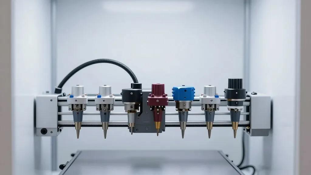
ASML Export Controls Push China Chipmakers to Costly Workarounds
China's chip producers are finding ways to manufacture advanced processors without the lithography tools they cannot buy, but each workaround brings higher costs and production risks.
By Rafael Ortega ·
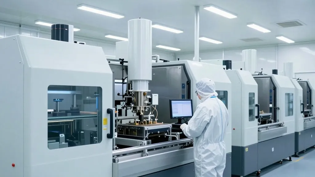
China's semiconductor manufacturers are navigating a critical hurdle: they cannot acquire the advanced extreme ultraviolet lithography machines that are essential for producing cutting-edge chips. Despite this, they are not at a complete standstill. Instead, they are relying on older deep ultraviolet equipment to produce capable silicon. The catch? This method introduces a cascade of challenges, including a higher potential for defects, longer production timelines, and mounting expenses, according to experts who spoke with Tom's Hardware.
Extreme ultraviolet technology has long been identified as the primary obstacle in China's ambition to develop cutting-edge processors. ASML is the sole manufacturer of these machines, which utilize 13.5nm-wavelength light to create some of the finest details on modern computer chips. Some analysts believe the gap between China and the West in this technology is five years or more.
Despite this restriction, China has achieved more than might have been expected. A 2023 examination of the Huawei Mate 60 Pro revealed its processor was manufactured by SMIC using a second-generation 7nm-class process without extreme ultraviolet tools. More recent analysis of the Kirin 9030 indicated SMIC had advanced its process closer to the density associated with 5nm manufacturing, though it still trails the leading processes from TSMC and Samsung.
The method used to achieve this progress involves a technique known as multiple patterning. Instead of printing an intricate layer in one pass, manufacturers split the design into several simpler patterns and build up the intended layer step by step. Chris Mack, co-founder and CTO of semiconductor firm Fractilia, said the question of whether a chip can be made without extreme ultraviolet ignores the trade-offs involved. He noted that industry wisdom held that three exposures on a 193 immersion tool cost about the same as one extreme ultraviolet exposure, but that at four masks extreme ultraviolet became the cheaper option. Quality is also at stake, as each new pattern must align precisely with what has already been etched, so more exposures mean more accumulated overlay errors and process variation. Designers can add space around features to compensate, but that enlarges the chip and reduces the number of dies per wafer, a costly outcome when wafers cost tens of thousands of dollars each. "You don't sell wafers, you sell die," Mack said.
Memory chips offer some evidence of the efficiency gap. In a June report, Morgan Stanley estimated Chinese DRAM maker CXMT produces only about one-third as many bits per wafer as Western rivals, and called lithography access a "hard ceiling" for Chinese memory development. Mack also cautioned that process "node" labels such as 5nm or 3nm have almost no meaning on their own, and SMIC's N+3 process, while progress, remains significantly less scaled than established 5nm processes from Samsung and TSMC. DUV still has room to run. Micron developed its 1-alpha DRAM without extreme ultraviolet, using multiple patterning and tight process control, and Mack said it "pushed 193 farther than any of the other memory makers did." Morgan Stanley considers CXMT's planned move to 1-alpha DRAM, intended for HBM3e, achievable without extreme ultraviolet. Copenhagen Business School researcher Douglas Fuller expects advanced packaging to let firms use DUV for the latest DRAM generations by the end of the decade. Mack added that China could go a long way if it had the full 193 immersion ecosystem and designed products around it, though he stressed that memory is much easier than logic.
Even Micron eventually turned to extreme ultraviolet for its 1-gamma DRAM, which it says delivers more than 30% greater bit density per wafer than the previous 1-beta generation. Extreme ultraviolet has its own drawbacks, including stochastic effects that can be countered with higher exposure doses, at greater cost. Still, Mack said he would be "hard pressed" to believe a 3nm or 2nm node could be economically viable without extreme ultraviolet tools.
That does not mean Chinese chipmakers will stall. They can keep pushing DUV while accepting larger dies, poorer yields, longer manufacturing times or a mix of the three, and they can add capacity. Morgan Stanley assumes CXMT stays on 1-alpha without extreme ultraviolet yet still lifts its share of global DRAM bit supply from 14% in 2026 to 16% in 2028 through new greenfield capacity. The bank also expects China's AI chip self-sufficiency to rise from 42% in 2025 to 70% by 2030, while extreme ultraviolet, HBM and advanced software leave a persistent gap.
As of this week, the situation remains unchanged. China's chipmakers continue to operate under export controls that block access to advanced lithography tools, and the trade-offs of working around those controls remain significant. The path forward for China's semiconductor industry will depend on how manufacturers balance the costs and risks of their current approach against their ambitions to catch up.
Source: Tom's Hardware